- 您现在的位置:买卖IC网 > Sheet目录2007 > MAX1080AEUP+ (Maxim Integrated Products)IC ADC 10BIT 400KSPS 20-TSSOP
MAX1080/MAX1081
Hardware Power-Down
Pulling SHDN low places the converter in hardware
power-down. Unlike software power-down mode, the
conversion is terminated immediately. When returning
to normal operation from SHDN with an external refer-
ence, the MAX1080/MAX1081 can be considered fully
powered up within 2s of actively pulling SHDN high.
When using the internal reference, the conversion
should be initiated only after the reference has settled;
its recovery time is dependent on the external bypass
capacitors and shutdown duration.
Power-Down Sequencing
The MAX1080/MAX1081 automatic power-down modes
can save considerable power when operating at less
than maximum sample rates. Figures 10 and 11 show
the average supply current as a function of the sam-
pling rate.
Using Full Power-Down Mode
Full power-down mode (FULLPD) achieves the lowest
power consumption, up to 1000 conversions per chan-
nel per second. Figure 10a shows the MAX1081’s
power consumption for one- or eight-channel conver-
sions utilizing full power-down mode (PD1 = PD0 = 0),
with the internal reference and the maximum clock
speed. A 0.01F bypass capacitor at REFADJ forms an
RC filter with the internal 17k
reference resistor, with a
200s time constant. To achieve full 10-bit accuracy,
seven time constants or 1.4ms are required after
power-up if the bypass capacitor is fully discharged
between conversions. Waiting this 1.4ms duration in
300ksps/400ksps, Single-Supply, Low-Power,
8-Channel, Serial 10-Bit ADCs with Internal Reference
16
______________________________________________________________________________________
PD1/PD0
MODE
CONVERTING
(mA)
AFTER
CONVERSION
INPUT COMPARATOR
REFERENCE
00
Full Power-Down
(FULLPD)
2.5
2A
Off
01
Fast Power-Down
(FASTPD)
2.5
0.9mA
Reduced Power
On
10
Reduced-Power
Mode (REDP)
2.5
1.3mA
Reduced Power
On
11
Normal Operating
2.5
2.0mA
Full Power
On
CIRCUIT SECTIONS*
TOTAL SUPPLY CURRENT
Table 4. Software-Controlled Power Modes
*Circuit operation between conversions; during conversion all circuits are fully powered up.
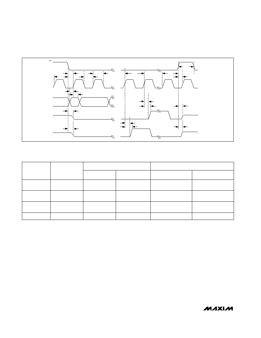
SCLK
DIN
DOUT
SSTRB
tCSS
tCH
tCSO
tCL
tDH
tDS
tDOE
tSTE
tCSW
tCP
tCSH
tCS1
tSTD
tDOD
tDOV
tDOH
tSTV
tSTH
CS
Figure 7. Detailed Serial-Interface Timing
发布紧急采购,3分钟左右您将得到回复。
相关PDF资料
MAX1084AESA+
IC ADC 10BIT 400KSPS 8-SOIC
MAX1093AEEG+
IC ADC 10BIT 250KSPS 24-QSOP
MAX1098CEAE+
IC ADC 10BIT SERIAL 16-SSOP
MAX11040GUU+T
IC ADC 24BIT 4CH 38-TSSOP
MAX11046ECB+T
IC ADC 16BIT PAR 250KSPS 64TQFP
MAX11046ETN+T
ADC 16BIT SAMPLING 8CH 56-TQFN
MAX11049ECB+
IC ADC 16BIT PAR 250KSPS 64TQFP
MAX1104EUA+
IC CODEC 8BIT 8-UMAX
相关代理商/技术参数
MAX1080AEUP+T
功能描述:模数转换器 - ADC Low-Power 8-Ch 10-Bit w/Int Ref RoHS:否 制造商:Texas Instruments 通道数量:2 结构:Sigma-Delta 转换速率:125 SPs to 8 KSPs 分辨率:24 bit 输入类型:Differential 信噪比:107 dB 接口类型:SPI 工作电源电压:1.7 V to 3.6 V, 2.7 V to 5.25 V 最大工作温度:+ 85 C 安装风格:SMD/SMT 封装 / 箱体:VQFN-32
MAX1080AEUP-T
功能描述:模数转换器 - ADC RoHS:否 制造商:Texas Instruments 通道数量:2 结构:Sigma-Delta 转换速率:125 SPs to 8 KSPs 分辨率:24 bit 输入类型:Differential 信噪比:107 dB 接口类型:SPI 工作电源电压:1.7 V to 3.6 V, 2.7 V to 5.25 V 最大工作温度:+ 85 C 安装风格:SMD/SMT 封装 / 箱体:VQFN-32
MAX1080BCUP
功能描述:模数转换器 - ADC Integrated Circuits (ICs) RoHS:否 制造商:Texas Instruments 通道数量:2 结构:Sigma-Delta 转换速率:125 SPs to 8 KSPs 分辨率:24 bit 输入类型:Differential 信噪比:107 dB 接口类型:SPI 工作电源电压:1.7 V to 3.6 V, 2.7 V to 5.25 V 最大工作温度:+ 85 C 安装风格:SMD/SMT 封装 / 箱体:VQFN-32
MAX1080BCUP+
功能描述:模数转换器 - ADC 5V 400ksps Low-Power 8Ch Serial 10-Bit RoHS:否 制造商:Texas Instruments 通道数量:2 结构:Sigma-Delta 转换速率:125 SPs to 8 KSPs 分辨率:24 bit 输入类型:Differential 信噪比:107 dB 接口类型:SPI 工作电源电压:1.7 V to 3.6 V, 2.7 V to 5.25 V 最大工作温度:+ 85 C 安装风格:SMD/SMT 封装 / 箱体:VQFN-32
MAX1080BCUP+T
功能描述:模数转换器 - ADC 5V 400ksps Low-Power 8Ch Serial 10-Bit RoHS:否 制造商:Texas Instruments 通道数量:2 结构:Sigma-Delta 转换速率:125 SPs to 8 KSPs 分辨率:24 bit 输入类型:Differential 信噪比:107 dB 接口类型:SPI 工作电源电压:1.7 V to 3.6 V, 2.7 V to 5.25 V 最大工作温度:+ 85 C 安装风格:SMD/SMT 封装 / 箱体:VQFN-32
MAX1080BCUP-T
功能描述:模数转换器 - ADC RoHS:否 制造商:Texas Instruments 通道数量:2 结构:Sigma-Delta 转换速率:125 SPs to 8 KSPs 分辨率:24 bit 输入类型:Differential 信噪比:107 dB 接口类型:SPI 工作电源电压:1.7 V to 3.6 V, 2.7 V to 5.25 V 最大工作温度:+ 85 C 安装风格:SMD/SMT 封装 / 箱体:VQFN-32
MAX1080BEUP
功能描述:模数转换器 - ADC RoHS:否 制造商:Texas Instruments 通道数量:2 结构:Sigma-Delta 转换速率:125 SPs to 8 KSPs 分辨率:24 bit 输入类型:Differential 信噪比:107 dB 接口类型:SPI 工作电源电压:1.7 V to 3.6 V, 2.7 V to 5.25 V 最大工作温度:+ 85 C 安装风格:SMD/SMT 封装 / 箱体:VQFN-32
MAX1080BEUP+
功能描述:模数转换器 - ADC 5V 400ksps Low-Power 8Ch Serial 10-Bit RoHS:否 制造商:Texas Instruments 通道数量:2 结构:Sigma-Delta 转换速率:125 SPs to 8 KSPs 分辨率:24 bit 输入类型:Differential 信噪比:107 dB 接口类型:SPI 工作电源电压:1.7 V to 3.6 V, 2.7 V to 5.25 V 最大工作温度:+ 85 C 安装风格:SMD/SMT 封装 / 箱体:VQFN-32